
Hands-on Projects for the Linux Graphics Subsystem
|

In a NutshellDevices like video cards need to map their video ram, where the contents are directed to the screen, and also their memory mapped I/O to the system memory. System memory includes therefore RAM addresses and device address space. Northbridge, the one part of the chipset (the other is Southbridge), is responsible to direct a given address either to RAM or to the device memory. In other words memory holes appear in ram to be used exclusively for device memory. Which part of the system memory is assigned to the device? Each PCI device maintains the PCI Configuration Space, which is a set of registers in the device. Some fields of this 'struct', called BARs, provide the amount of memory that the device requires. The BIOS (or the Operating System in some cases) is responsible to look for the required memory area of all PCI devices (by reading in a certain way the BAR) then and then write back to the BARs the starting system memory address that the device address space should be placed so that conflicts with other devices is avoided. It is the turn of the Operating System then to read the BAR values filled previously and inform the device drivers about the exact locations of the device memory they handle. There are two ways to access the PCI Configuration space and the BARs. For 16-bit systems, I/O ports and interrupt 0x1a. For 32-bit protected mode systems there is another way, Bios32, which calls a function, which resides in the PCI BIOS (somewhere bellow the first 1 MB of the PC system memory).
|
General info about PCI is provided by this Wikipedia article. From PCI bus info and code we read:
|
There are 4 components to the PCI subsytem: Bus Number Device Number Function Number Register Number There are up to 256 available Buses on a PCI system, most commonly all the cards and chips will be located on Bus 0 and Bus 1. When scanning for hardware, it's a good idea to scan all 256 buses as it won't take that much additional time. A Device is a physical thing on the PCI bus. It could be a video card, an ethernet card, a Northbridge, anything. There is a software maximum of 32 devices that can exist on each bus. The physical hardware limit is much lower than this due to electrical loading issues, but we won't get into that. Devices on a motherboard are typically scattered throughout the 32 devices, holes can and will exist. Your software must scan all 32 devices on each bus. All devices have at least 1 function. Multi-function devices, such as a combination modem/soundcard will usually have 2 devices, typically numbered 0 and 1. There are 8 possible functions per device, numbered 0-7. Any device that has more than 1 function is (hey clever!) called a multi-function device. Functions start numbering at 0 and work up to 7. Every function of a device has 256 eight-bit registers. Registers 0-3F are defined by the PCI specification and provide a wealth of information about the particular function. Registers 40-FF are vendor defined and control the properties of the function itself. Without vendor specific documentation, these registers should probably be left untouched. |
Notice that the Bus, Device, Function triplet mentioned previously is the Bus ID we find in the configuration file xorg.conf. From the xorg.conf man page we read:
|
BusID "bus-id" This specifies the bus location of the graphics card. For PCI/AGP cards, the bus-id string has the form PCI:bus:device:function (e.g., "PCI:1:0:0" might be appropriate for an AGP card). This field is usually optional in single-head configurations when using the primary graphics card. In multi-head configurations, or when using a secondary graphics card in a single-head configuration, this entry is mandatory. Its main purpose is to make an unambiguous connection between the device section and the hardware it is representing. This information can usually be found by running the Xorg server with the -scanpci command line option. |
As we read in Linux Plug-and-Play HOWTO:
|
There are three types of addresses: main memory addresses, I/O addresses (ports) and configuration addresses. On the PCI bus, configuration addresses constitute a separate address space just like I/O addresses do. To access both I/O and (main) memory address "spaces" the same address bus is used (the wires used for the address are shared). How does the device know whether or not an address which appears on the address bus is a memory address or I/O address? Well, for ISA (for PCI read this too), there are 4 dedicated wires on the bus that convey this sort of information. If a certain one of these 4 wires is asserted, it says that the CPU wants to read from an I/O address, and the main memory ignores the address on the bus. In all, read and write wires exist for both main memory and I/O addresses (4 wires in all). For the PCI bus it's the same basic idea (also using 4 wires) but it's done a little differently. Instead of only one of the four wires being asserted, a binary number is put on the wires (16 different possibilities). Thus, more info may be conveyed by these 4 wires.. Four of these 16 numbers serve the I/O and memory spaces as in the above paragraph. In addition there is also configuration address space which uses up two more numbers. This leaves 10 more numbers left over for other purposes.
|
From Motherboard Chipsets and the Memory Map we read:
|
We're used to thinking of memory only in terms of RAM, the stuff programs read from and write to all the time. And indeed most of the memory requests from the processor are routed to RAM modules by the northbridge. But not all of them. Physical memory addresses are also used for communication with assorted devices on the motherboard (this communication is called memory-mapped I/O).
When the northbridge receives a physical memory request it decides where to route it: should it go to RAM? Video card maybe? This routing is decided via the memory address map. For each region of physical memory addresses, the memory map knows the device that owns that region. The bulk of the addresses are mapped to RAM, but when they aren't the memory map tells the chipset which device should service requests for those addresses.  |
 |
For the same point we read from Memory Hole in Large Memory X86 Based Systems:
|
In the X86 architecture, there are 2 types of devices that are mapped into processor
address space. The first type is physical memory. There is a 1:1 correlation between
memory size and processor address space. A system with 512MB of physical memory
will require 512MB of processor address space for it to be accessed.
The second, and perhaps less obvious, type is device memory or device address space. This gets complex because there are many different types of devices. For simplicity, and purpose of this paper, we will focus on common devices such as AGP and PCI cards. Take for example a graphics card with 128MB of video memory. This is dedicated device memory that is used to store video data displayed on the screen. Video memory must be accessible by the processor and therefore mapped into processor address space. This means that the graphics card will require 128MB of processor address space. It is important to understand that both physical memory and device memory require processor address space. I used the graphics card example above but remember that there are devices that do not have memory, which require address space as well.
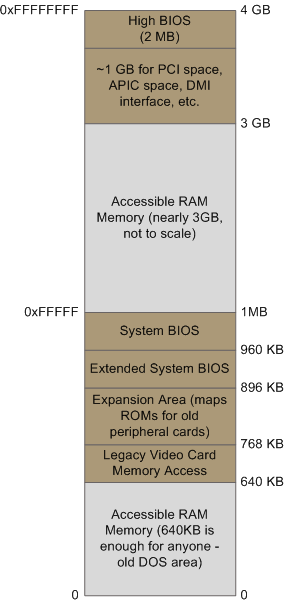
The device address space hole (aka the PCI hole)The problem arises when the amount of physical memory plus the amount of device memory exceeds the processors address space. Software running on 32-bit processors is constrained to 32-bits of address space. This means that there is a general limit of 4 GB (2^32) for memory and device address space. Let's take a look at a typical 32-bit address map in a machine with 1GB of memory.
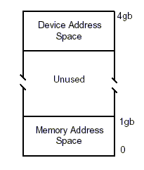 As you can see, there is plenty space within the processors 32-bit address range to accommodate both physical memory and device address spaces. Note that this is a simplistic representation of a memory map. Kernels can, and do, map memory in different places. As a result, a system with 1GB of physical memory will not loose any memory because of the required device address space. When you add 4GB of memory in a 32-bit system, you get this:
 In this configuration, the address space for physical memory and device memory overlap causing a conflict. This will not work because 2 devices can't occupy the same address space. The only way to resolve this conflict (and retain compatibility) is to allow the device address space to be mapped over the memory causing a hole in this address range.
|
The actual address that a PCI device uses, e.g. for the video card its frame buffer and also its MMIO addresses, are provided by the BIOS at boot time or by the OS itself. BIOS checks the BAR field of the PCI Configuration space (see bellow) for the specific memory location. In some cases for instance a conflict between two PCI cards the BIOS can also alter the BAR values. As the previous figures denote and also as explained in Memory over 3GB on NetWare PCI devices use the system space between 3 GB and 4 GB for framebuffer and MMIO memory:
| Another feature of the x86 architecture is device memory. PCI devices, such as network cards and SCSI and FibreChannel cards, reserve memory at the top of the 4GB range for their own use. This is done in hardware to facilitate I/O to the devices. The side-effect of this is that not all of the 4GB space is usable by the operating system for running programs. |
Also from Linux Device Drivers we read:
|
When power is applied to a PCI device, the hardware remains inactive. In other words, the device will respond only to configuration transactions. At power on, the device has no memory and no I/O ports mapped in the computer's address space; every other device-specific feature, such as interrupt reporting, is disabled as well.
Fortunately, every PCI motherboard is equipped with PCI-aware firmware, called the BIOS, NVRAM, or PROM, depending on the platform. The firmware offers access to the device configuration address space by reading and writing registers in the PCI controller. At system boot, the firmware (or the Linux kernel, if so configured) performs configuration transactions with every PCI peripheral in order to allocate a safe place for any address region it offers. By the time a device driver accesses the device, its memory and I/O regions have already been mapped into the processor's address space. The driver can change this default assignment, but it will never need to do that. |
The two regions of device address space that need to be mapped in system memory are the Framebuffer and the MMIO.
Certainly each device type needs memory for different purposes. For instance a network card needs device memory space as the buffer that stores the packets that sends or receives. For the video card this space is the framebuffer. We have already met in this site framebuffer, the memory area that is mapped in the video ram (see X.Org Wiki).
Other than the video ram the video cards (and also other types of cards) need also system memory for MMIO assignments. From this Wikipedia article we read:
|
Memory-mapped I/O (MMIO) and port I/O (also called port-mapped I/O or PMIO) are two complementary methods of performing input/output between the CPU and peripheral devices in a computer.
Memory-mapped I/O uses the same address bus to address both memory and I/O devices, and the CPU instructions used to access the memory are also used for accessing devices. Port-mapped I/O uses a special class of CPU instructions specifically for performing I/O. This is generally found on Intel microprocessors, specifically the IN and OUT instructions which can read and write one to four bytes (outb, outw, outl) to an I/O device. |
One reason for using MMIO for PCI cards is to control them via the card registers. Those registers are also mapped to system memory. From this xorg wiki we read:
| 2D engines are usually either controlled via direct MMIO access to the relevant registers or via a command queue. With direct MMIO, the appropriate values are written the relevant registers and then the command is usually executed when the last reg in the series is written or when the command register is written (depends on HW). With a command queue, part of the framebuffer is reserved as a command queue (FIFO). Commands and associated data are written sequentially to the queue and processed via the drawing engine. |
From PCI we read:
|
PCI I/O and PCI Memory Addresses
These two address spaces are used by the devices to communicate with their device drivers running in the Linux kernel on the CPU. For example, the DECchip 21141 fast ethernet device maps its internal registers into PCI I/O space. Its Linux device driver then reads and writes those registers to control the device. Video drivers typically use large amounts of PCI memory space to contain video information |
The source code of the framebuffer and mmio mapping to the system memory, for the current thread we follow in this site, is provided in MGAMapMem(). This function has the comment "Map the framebuffer and MMIO memory".
In the following sections we see that the exact positions of the system memory used are indicated by the BAR fields of the PCI Configuration space.
As we read in Linux Plug-and-Play HOWTO:
|
This is different from the IO and memory address spaces because configuration address space is "geographic". Each slot for a card has the slot number as part of the address. This way, Linux (or the BIOS) can address a certain slot and find out what type of card is in that slot. Each device has 64 standard byte-size registers and some of these hold numbers which can unambiguously identify the device. Since the number of slots is limited as are the number of PCI devices built into motherboard, Linux (or the BIOS) only needs to check a limited number of addresses to find all the PCI devices. If it reads all ones (0xFF in hexadecimal) from the first register of a device, then that means that no device is present. Since there is no card or device to supply all these ones (0xFF) number, the PCI "host bridge" on the motherboard supplies (spoofs) this number for all non-existent device. The PCI slot number is called (in PCI lingo) the "Device Number" and since a card may have up to 8 devices on it, a "Function Number" from 0-7 identifies which device it is on a PCI card. These numbers are part of the geographic address. Linux programmers call it "pci-slot-name". Thus what Linux calls a "device" is actually a "function" in PCI lingo. The PCI bus number (often 00) also becomes part of the geographic address. For example, 0000:00:0d.2 is PCI bus 0, slot 0d, function 2. For the full geographic address, one must include the double-word number of the device's configuration registers which one wants to access. The leading 0000 (in 1999) were reserved for future use. How does the CPU designate that a read or write is to a PCI configuration space? It doesn't, at least not directly. Instead when access to configuration space is desired it does a 32-bit (double-word) write to 0cf8-0cfb in I0 space and writes the full geographic address there. The PCI host bridge is listening at this address and insures that any next write of data to 0cfc-0cff is put into the specified configuration registers of the specified device. The bridge does this both by sending a special signal to the specified PCI card (or the like) on a dedicated wire that goes only to the slot where the card is plugged in. It also puts bits on the control bus saying that what's on the address bus now is a geographic configuration space address. Why not make it simple and just have the CPU put bits on the control bus to say that the address on the main bus is a geographic one for PCI configuration? Well, most CPU's are not capable of doing this so the PCI host bridge gets to do it instead. |
As mentioned previously each PCI device is required to provide its PCI configuration space. This is provided by the 256-byte Configuration registers of the device and has the following form:
| register | bits 31-24 | bits 23-16 | bits 15-8 | bits 7-0 |
|---|---|---|---|---|
| 00 | Device ID | Vendor ID | ||
| 04 | Status | Command | ||
| 08 | Class code | Subclass | Prog IF | Revision ID |
| 0C | BIST | Header type | Latency Timer | Cache Line Size |
| 10 | Base address #0 (BAR0) | |||
| 14 | Base address #1 (BAR1) | |||
| 18 | Base address #2 (BAR2) | |||
| 1C | Base address #3 (BAR3) | |||
| 20 | Base address #4 (BAR4) | |||
| 24 | Base address #5 (BAR5) | |||
| 28 | Cardbus CIS Pointer | |||
| 2C | Subsystem ID | Subsystem Vendor ID | ||
| 30 | Expansion ROM base address | |||
| 34 | Reserved | Capabilities Pointer | ||
| 38 | Reserved | |||
| 3C | Max latency | Min Grant | Interrupt PIN | Interrupt Line |
From tech-pro.net we read:
| Each PCI device has a block of 256 bytes of configuration space: 16 32-bit doublewords of header information plus 48 doublewords of device-specific configuration registers. |
From this Wikipedia article we read:
|
The Vendor ID and Device ID registers identify the device, and are commonly called the PCI ID. The 16-bit vendor ID is allocated by the PCI SIG. The 16-bit device ID is then assigned by the vendor. There is an ongoing project to collect all known Vendor and Device IDs.
The Subsystem Vendor ID and the Subsystem Device ID further identify the device. The Vendor ID is that of the chip manufacturer, and the Subsystem Vendor ID is that of the card manufacturer. The Subsystem Device ID is assigned by the subsystem vendor, but is assigned from the same number space as the Device ID. The Status register is used to report which features are supported and whether certain kinds of error have occurred. The Command register contains a bitmask of features that can be individually enabled and disabled. The Cache Line Size register must be programmed before the device is told it can use the memory-write-and-invalidate transaction. This should normally match the CPU's cache line size, but the correct setting is system dependent. |
From this Wikipedia article we read:
| Each non-bridge PCI device can implement up to 6 BARs, each of which can respond to different addresses in I/O port and memory mapped address space. |
From PCI OSDev page we read:
|
Base address Registers (or BARs) can be used to hold memory addresses used by the device, or offsets for port addresses. Typically, memory address BARs need to be located in physical ram while I/O space BARs can reside at any memory address (even beyond physical memory). To distinguish between them, you can check the value of the lowest bit. The following tables describe the two types of BARs:
|
Byte 3 of the Memory Space BAR Layout indicates a Prefetchable or non-Prefetchable memory. From The PCI Interface we read:
|
Accessing the I/O and Memory Spaces
A PCI device implements up to six I/O address regions. Each region consists of either memory or I/O locations. Most devices implement their I/O registers in memory regions, because it's generally a saner approach. However, unlike normal memory, I/O registers should not be cached by the CPU because each access can have side effects. The PCI device that implements I/O registers as a memory region marks the difference by setting a "memory-is-prefetchable" bit in its configuration register. If the memory region is marked as prefetchable, the CPU can cache its contents and do all sorts of optimization with it; nonprefetchable memory access, on the other hand, can't be optimized because each access can have side effects, just as with I/O ports. Peripherals that map their control registers to a memory address range declare that range as nonprefetchable, whereas something like video memory on PCI boards is prefetchable. In this section, we use the word region to refer to a generic I/O address space that is memory-mapped or port-mapped. |
We previously saw that a certain BAR field of a PCI device is assigned either to a memory or to a I/O value. From the BAR we can retrieve: i. the size of the memory the specific value requires and ii. the actual starting location in the memory.
Again from PCI OSDev page we read:
|
When you want to retrieve the actual base address of a BAR, be sure to mask the lower bits. For 16-Bit Memory Space BARs, you calculate (BAR[x] & 0xFFF0). For 32-Bit Memory Space BARs, you calculate (BAR[x] & 0xFFFFFFF0). For 64-Bit Memory Space BARs, you calculate ((BAR[x] & 0xFFFFFFF0) + ((BAR[x+1] & 0xFFFFFFFF) << 32)) For I/O Space BARs, you calculate (BAR[x] & 0xFFFFFFFC). To determine the amount of address space needed by a PCI device, you must save the original value of the BAR, write a value of all 1's to the register, then read it back. The amount of memory can then be determined by masking the information bits, performing a logical NOT, and incrementing the value by 1. The original value of the BAR should then be restored. The BAR register is naturally aligned and as such you can only modify the bits that are set. For example, if a device utilizes 16 MB it will have BAR0 filled with 0xFF000000 (0x01000000 after decoding) and you can only modify the upper 8-bits. |
As we previously saw each PCI device has six BARs that describe the address spaces of the device. When the sequence of 1s are written to the register and the BAR is read back bit 0 describes an I/O or a memory BAR. Bits 1-3 are also reserved. For the remaining bits starting from the less significant, the first 1 that we encounter determines the size of the memory space. For instance if we read back FFF00000, which the binary value:
the following assumptions are made:
It is a memory address space (bit 0 =0)
It is a 32-bit memory address (bits 1,2 = 00)
This memory space has 1 MB size since the first 1 we meet at bit 20 indicates the binary value:
which is decimal 1 MB.
We previously examined the info that results from the BAR registers of the PCI configuration space. This info concerned the total size of the memory required by the device. We saw that the method to find that required a write 1a and read back operation and then restoring the initial value. This value shows exactly the starting location in the memory or I/O space. By combining the starting address with the total size we have the whole description of the memory a PCI device requires. The exact location is not hardwired and is up to the responsible program that sets up the PCI to find a right place, usually from 3 GB to 4GB that certainly does not conflict with the memory of other devices.
The question however is which part of the system software sets the exact values into the BARs. Usually the firmware (e.g. BIOS) or in some cases the Operating System is appointed to fill the BARs of the system devices with values that take in account the size of the memory areas that the PCI devices require and the starting address, certainly in a way that collisions between two areas are avoided.
From System Configuration and the PCI BIOS we read:
| But, having said that the BIOS can configure the PCI hardware doesn't necessarily mean that it will. Later Windows operating systems incorporate full Plug-and-Play capability and are referred to as PnP operating systems. Even if the BIOS does the configuration, the OS may go ahead and do its own configuration when it is started. The BIOS will typically have a parameter called "PnP OS Installed." If this parameter is set to "Yes," the BIOS will skip PCI configuration beyond the minimum necessary to boot the operating system. |
From Linux Device Drivers we read:
| At system boot, the firmware (or the Linux kernel, if so configured) performs configuration transactions with every PCI peripheral in order to allocate a safe place for any address region it offers. By the time a device driver accesses the device, its memory and I/O regions have already been mapped into the processor's address space. The driver can change this default assignment, but it will never need to do that. |
As we also read from PCI Subsystem:
| On all IBM PC-compatible machines, BARs are assigned by the BIOS. Linux simply scans through the buses and records the BAR values. |
The same page shows some ways to intervene to the BIOS assignment of the BARs. This means that read and write operations for the PCI configuration space should be provided for the Operating Systems as discussed next.
Also from Linux Kernel we read about the PCI Fixup code, i.e. the code that configures PCI memory locations, I/O values and interrupt lines:
|
PCI Fixup
The PCI fixup code for Alpha AXP does rather more than that for Intel (which basically does nothing). For Intel based systems the system BIOS, which ran at boot time, has already fully configured the PCI system. This leaves Linux with little to do other than map that configuration. For non-Intel based systems further configuration needs to happen to:
* Allocate PCI I/O and PCI Memory space to each device, |
Also from PCI we read:
|
Aligns the current global PCI I/O and Memory bases on 4K and 1 Mbyte boundaries respectively,
For every device on the current bus (in ascending PCI I/O memory needs),
* allocates it space in PCI I/O and/or PCI Memory,
Allocates space recursively to all of the buses downstream of the current bus. Note that this will change the global PCI I/O and Memory bases |
The video driver as we examine in section 3.2.2.11 uses the BAR information, stored at boot time by the BIOS, and retrieved by the Operating System. This info can either be memory location or I/O address used by the video card.
Who needs to access the configuration space? Usually the Operating System needs to provide the device drivers with info about the memory they handle. From PCI drivers we read:
| After the driver has detected the device, it usually needs to read from or write to the three address spaces: memory, port, and configuration. In particular, accessing the configuration space is vital to the driver, because it is the only way it can find out where the device is mapped in memory and in the I/O space. |
From tech-pro.net we read:
|
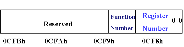
Configuration space is completely separate from memory and I/O space, and can only be accessed using the PCI bus Configuration Read and Write commands. Intel x86 processors cannot access configuration space directly, so the PCI specification defines two methods by which this can be achieved. The preferred method, used by current implementations, is to write the target address to the 32-bit I/O port at 0CFBh, and then read or write the doubleword through I/O port 0CFCh. A second method, used by early PCI chip sets but now discouraged by the PCI specification, involves using I/O ports at 0CF8h and 0CFAh to map the configuration spaces of up to 16 PCI devices into the I/O range C000h to CFFFh, from where the data may be read or written.
The above information was given for interest only. The correct way for software such as device drivers or diagnostic programs to access a device's configuration space is using the functions provided in the PCI BIOS. The PCI BIOS function code is 0B1h. If a program calls interrupt 1Ah with the AX register set to 0B101h the carry bit will be clear on return if the PCI BIOS is present, and the 32-bit EDX register will contain the ASCII characters " PCI." Register BX will contain the major and minor BIOS revision version. Register AL will be odd (bit 0 set) if the system supports the preferred configuration space addressing mechanism. Using other subfunctions of BIOS function 0B1h programs can search for a device and obtain its location, find devices of a particular class, read and write to configuration space, generate a PCI bus special cycle, discover how PCI interrupts have been assigned to IRQ lines, and set a PCI device's interrupt to a particular IRQ. Normally, of course, these functions would only be carried out by system software. |
In this text we see again the 1st method of accessing the configuration space (via the 0CFBh, 0CFCh I/O ports) however here it suggests the 2nd method via the interrupt 1Ah, which is the method for Operating Systems running in Real Mode. For Protected mode the PCI BIOS is used.
This text from OSDev describes the 1st configuration method:
|
Configuration Mechanism #1
Two 32-bit I/O locations are used, the first location (0xCF8) is named CONFIG_ADDRESS, and the second (0xCFC) is called CONFIG_DATA. CONFIG_ADDRESS specifies the configuration address that is required to be accesses, while accesses to CONFIG_DATA will actually generate the configuration access and will transfer the data to or from the CONFIG_DATA register. The CONFIG_ADDRESS is a 32-bit register with the format shown in following figure. Bit 31 is an enable flag for determining when accesses to CONFIG_DATA should be translated to configuration cycles. Bits 23 through 16 allow the configuration software to choose a specific PCI bus in the system. Bits 15 through 11 select the specific device on the PCI Bus. Bits 10 through 8 choose a specific function in a device (if the device supports multiple functions). Bits 7 through 2 select the specific 32-bit area in the device's configuration space.
The following code segment illustrates the use of configuration mechanism #1. Note that this segment, the functions sysOutLong and sysInLong are assembly language functions that make use of the OUTL and INPL Pentium assembly language instructions.
When a configuration access attempts to select a device that does not exist, the host bridge will complete the access without error, dropping all data on writes and returning all ones on reads. |
Notice that the four values that are highlighted in the CONFIG_ADDRESS are the components to the PCI subsytem described in the start of the current page, section 'What is PCI'.
Also the code snippet included is straightforward since it completes the configuration address by left-shofting values in their appropriate position. The value:
(UINT32)0x80000000
is the decimal value:
10000000000000000000000000000000
which sets the 'Enable' bit.
Also hex value 0xfc is decimal 11111100 which zeroes bits 0 and 1.
To initialize the device an address space should be assigned to this device. WE previously saw that this space can be either memory or I/O space or both. The software that fixes up the devices memory can access the host/PCI bridge through the CONFIG_DATA and CONFIG_ADDRESS I/O locations.
We previously saw that the Configuration Address Register at 0CF8h has the form:

This register selects the PCI bus, the device on the bus, the function of the device (configuration space) and the specific register inside the configuration space. Through the host/PCI bridge this request is translated to the following address on the specific bus:
This address selects the specific device on the bus. To do this the IDSEL pin is used. This pin selects a device which is found in a specific slot 'geographically'. The pin is asserted by the use of a decoder that can be used according to the PCI memory controller in the following ways (see Linux Kernel: PCI):
a. Only one bit can be '1' in the area 31:11. Each bit corresponds to a different slot. In this case bit 11 would select the device in slot 0, bit 12 in the device slot 1, etc. In this case only 21 device are supported per bus instead of 32, the PCI specification states.
b. The slot number is written directly in bits 31:11

After the initialization is complete the device can be handled via the memory and I/O space.
From this Linux PCI page we read about the PCI BIOS:
| The PCI BIOS functions are a series of standard routines which are common across all platforms. For example, they are the same for both Intel and Alpha AXP based systems. They allow the CPU controlled access to all of the PCI address spaces. |
The PCI BIOS Specification and PCI Special Interest Group documents provide a thorough description of the PCI BIOS functions of the interrupt 0x1A. From the former we read:
|
Access to the PCI BIOS functions for 16-bit callers is provided through Interrupt 1Ah.
32-bit (ie. protect mode) access is provided by calling through a 32-bit protect mode entry
point. The PCI BIOS function code is B1h. Specific BIOS functions are invoked using a
subfunction code. A user simply sets the host processors registers for the function and
subfunction desired and calls the PCI BIOS software. Status is returned using the Carry
flag ([CF]) and registers specific to the function invoked.
The PCI BIOS provides a 16-bit real and protect mode interface and a 32-bit protect mode interface. The 16-bit interface is provided through PC/AT Int 1Ah software interrupt. The PCI BIOS Int 1Ah interface operates in either real mode, virtual-86 mode, or 16:16 protect mode. The BIOS functions may also be accessed through the industry standard entry point for INT 1Ah (physical address 000FFE6Eh) by simulating an INT instruction1. The INT 1Ah entry point supports 16-bit code only. Protect mode callers of this interface must set the CS selector base to 0F000h. The protected mode interface supports 32-bit protect mode callers. The protected mode PCI BIOS interface is accessed by calling (not a simulated INT) through a protected mode entry point in the PCI BIOS. The entry point and information needed for building the segment descriptors are provided by the BIOS32 Service Directory (see section 3.3). 32- bit callers invoke the PCI BIOS routines using CALL FAR.
|
Therefore to read a word from the configuration space function PCI_FUNCTION_ID (B1h) with subfunction READ_CONFIG_DWORD (0Ah) is implemented:
|
4.3.3. Read Configuration Dword This function allows reading individual dwords from the configuration space of a specific device. The Register Number parameter must be a multiple of four (i.e., bits 0 and 1 must be set to 0).
ENTRY: [AH] PCI_FUNCTION_ID [AL] READ_CONFIG_DWORD [BH] Bus Number (0...255) [BL] Device Number in upper 5 bits, Function Number in lower 3 bits [DI] Register Number (0,4,8,...252) EXIT: [ECX] Dword read. [AH] Return Code: SUCCESSFUL BAD_REGISTER_NUMBER [CF] Completion Status, set = error, reset = success |
As with the first configuration method the four values that are highlighted are the components to the PCI subsytem described in the start of the current page, section 'What is PCI'.
It also describes the BIOS32 Service Directory, which detects and provides the 32-bit PCI BIOS services, as:
|
The description of this mechanism, known as
BIOS32 Service Directory, is provided in three parts; the first part specifies an algorithm
for determining if the BIOS32 Service Directory exists on a platform, the second part
specifies the calling interface to the BIOS32 Service Directory, and the third part
describes how the BIOS32 Service Directory supports PCI BIOS detection.
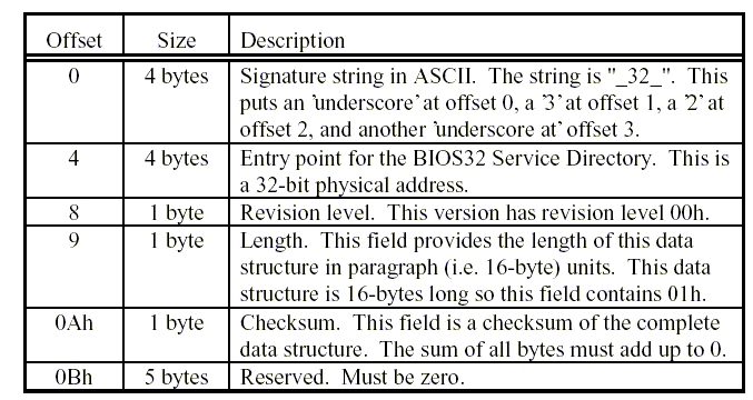
A BIOS which implements the BIOS32 Service Directory must embed a specific, contiguous 16-byte data structure, beginning on a 16-byte boundary somewhere in the physical address range 0E0000h - 0FFFFFh. A description of the fields in the data structure are given in Table 3.1.
 Clients of the BIOS32 Service Directory should determine its existence by scanning 0E0000h to 0FFFF0h looking for the ASCII signature and a valid, checksummed data structure. If the data structure is found, the BIOS32 Service Directory can be accessed through the entry point provided in the data structure.
|